This converter makes it possible to determine the characteristic impedance Z₀ and the propagation delay of a microstrip line as a function of its dimensions and the relative dielectric constant of the substrate. It uses empirical corrections and Hammerstad’s formulas to provide accurate results suitable for RF and PCB designs.
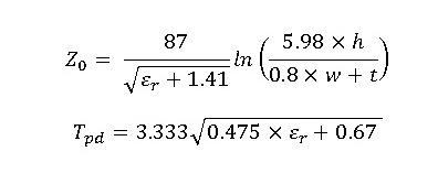
Formula
Δ raw = t × (1 + 1/ε r ) / (2π) × ln(4e / √( (t/H)² + (1/π)² / ( (W/t) + 1.1)² ))
W eff = W + Δ raw × factor
ε eff = function(H, W eff , ε r )
Z₀ = function(ε eff , W eff , H)
TD = √(ε eff ) / c × factor
Explanation of the formula
The Δ raw correction adjusts the effective width of the line to compensate for the thickness of the trace. The effective width W eff is then used to calculate the effective permittivity ε eff via the Hammerstad formula. The impedance Z₀ is derived from ε eff and W eff . Finally, the propagation delay TD expresses the propagation speed of the signal through the microstrip line.
Uses
- Sizing microstrip lines for RF and high frequency applications.
- Evaluate the effect of dimensions and dielectric constant on characteristic impedance.
- Optimize PCB designs to minimize losses and reflections.
- Ensure precise matching between lines and components for efficient signal transfer.